1
/
of
3
Xilinx Zynq UltraScale+ MPSoC FPGA Development Board ADK-19
Xilinx Zynq UltraScale+ MPSoC FPGA Development Board ADK-19
Regular price
$13,518.00 USD
Regular price
Sale price
$13,518.00 USD
Shipping calculated at checkout.
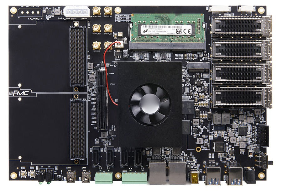
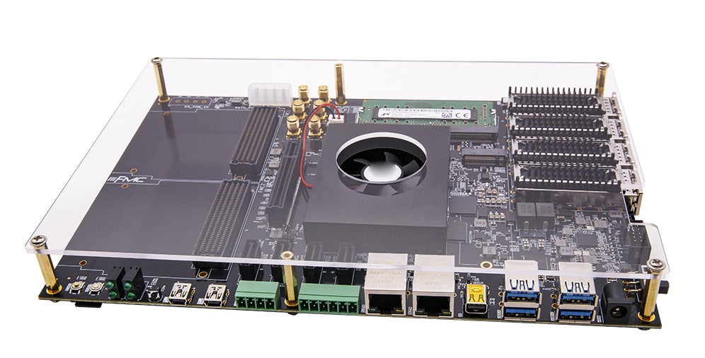
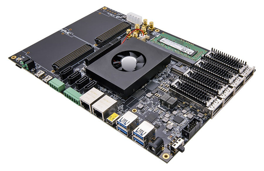
The ADK-19 is a flagship FPGA development board built around the Xilinx Zynq UltraScale+ MPSoC device XCZU19EG-2FFVC1760I, combining a quad-core ARM Cortex-A53 processing system with a dual-core Cortex-R5 real-time processor, a Mali-400 MP2 GPU and large-scale programmable logic. With 8GB of DDR4 memory, 32GB eMMC and 128MB QSPI flash storage, four 100G QSFP28 optical ports and two FMC HPC expansion connectors, it supports the Xilinx Vitis-AI DPU and targets high-speed optical networking, high-speed data exchange and storage, industrial control, deep learning and AI, cloud computing and 4K video transmission and processing. Development software: Vitis 2020.1; Linux: PetaLinux 5.4.0 (2020.1).
Specifications
| Item | Specification |
|---|---|
| FPGA device | XCZU19EG-2FFVC1760I |
| CPU | 4x ARM Cortex-A53, 1.333 GHz; 2x ARM Cortex-R5, 533 MHz |
| GPU | Mali-400 MP2 |
| Device grade | Speed grade -2, industrial grade, operating temperature -40 °C to +85 °C |
| PS high-speed connectivity | PCIe Gen2 x4, 2x USB 3.0, SATA 3.1, DisplayPort, 4x Tri-mode Gigabit Ethernet |
| PS general connectivity | 2x USB 2.0, 2x SD/SDIO, 2x UART, 2x CAN 2.0B, 2x I2C, 2x SPI, 4x 32-bit GPIO |
| Logic cells | 1,143K |
| Flip-flops | 1,045K |
| LUTs | 523K |
| Global clocks (CMTs) | 11 |
| DSP slices | 1,968 |
| Max. distributed RAM | 9.8 Mb |
| Total Block RAM | 34.6 Mb |
| UltraRAM | 36 Mb |
| PCIe (PL) | PCIe Gen3 x16 |
| 100G Ethernet | 4 |
| 150G Interlaken | 4 |
| PL GTY transceivers | 16x 28.21 Gb/s |
| PL GTH transceivers | 32x 16.3 Gb/s |
| DDR4 memory | PS side: 4x 2GB DDR4 chips, 8GB total, 64-bit, 2400 Mbps; PL side: 260-pin DDR4 SODIMM slot (memory module not included) |
| QSPI flash | 2x 64MB QSPI flash, 128MB total, for U-Boot, system files and user data |
| eMMC flash | 1x 32GB eMMC on the PS side, for the operating system and user data |
| PCIe slot | 1x PCIe x8 slot for PCIe x8/x4/x2/x1 cards, PCI Express 3.0, up to 8 Gb/s per lane |
| DisplayPort output | 1x DisplayPort output, up to 4K@30Hz or 1080P@60Hz |
| 100G optical ports | 4x QSFP28 optical ports with independent transmit and receive channels, 100 Gb/s per port |
| FMC expansion | 2x FMC HPC expansion connectors for FMC daughter cards (HDMI input/output modules, binocular camera modules, high-speed AD modules, etc.) |
| CAN | 2x CAN bus interfaces |
| RS485 | 2x RS485 interfaces |
| MIPI | 1x MIPI camera input interface |
| M.2 NVMe | 1x PCIe x1 M.2 NVMe slot for an M.2 NVMe SSD (SSD not included) |
| USB-to-UART | 1x UART-to-USB for the PS and 1x for the PL, for PC communication and debugging; a third UART is routed from the PS via a 1mm-pitch 10-pin FPC connector |
| Ethernet | 1x Gigabit Ethernet on the PL side and 1x on the PS side |
| USB 3.0 | 4x USB 3.0 ports |
| SMA | 3 pairs of differential SMA connectors for high-speed input/output signals |
| SATA | 4x SATA ports |
| JTAG | 10-pin 2.54mm standard JTAG port, for FPGA program download and debugging |
| Clock configuration | 32.768 kHz crystal as the PS real-time clock source; 33.333 MHz oscillator for the PS; 200 MHz differential clock for the PL system and as the DDR4 controller reference clock |
| Real-time clock | 1x built-in RTC |
| EEPROM | 1x I2C EEPROM 24LC04 |
| Temperature sensor | LM75, for ambient temperature detection |
| SD slot | 1x Micro SD card slot |
| LEDs | 1x power indicator, 1x DONE configuration indicator, 2x user LEDs |
| Buttons | 1x reset button, 2x user buttons |
| Power input | +12V input; 12V / 5A supply; 5A maximum input current |
| Dimensions | 250 mm x 170 mm |
| PCB | 8-layer PCB design, with dedicated power and GND planes |
What’s in the box
- FPGA development board x 1
- Cooling fan x 1
- Mini USB cable x 1
- USB downloader x 1
- 12V power supply x 1
- Transparent protective plate x 1
- TF (Micro SD) card x 1
- Card reader x 1
Share