Xilinx Zynq-7000 XC7Z020 + TI LMK04828 Clock Synchronization Board ADK-W104
Xilinx Zynq-7000 XC7Z020 + TI LMK04828 Clock Synchronization Board ADK-W104
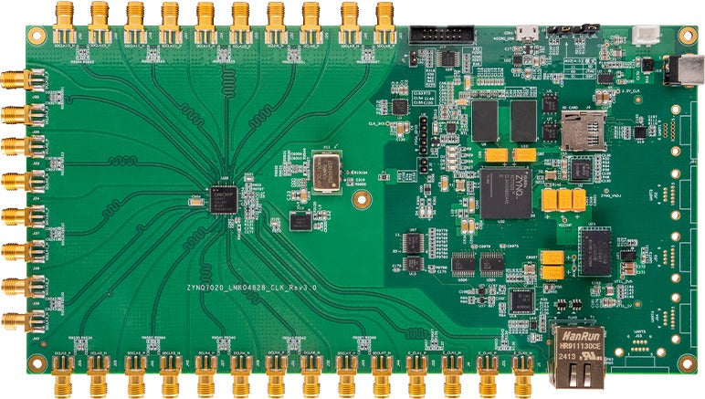
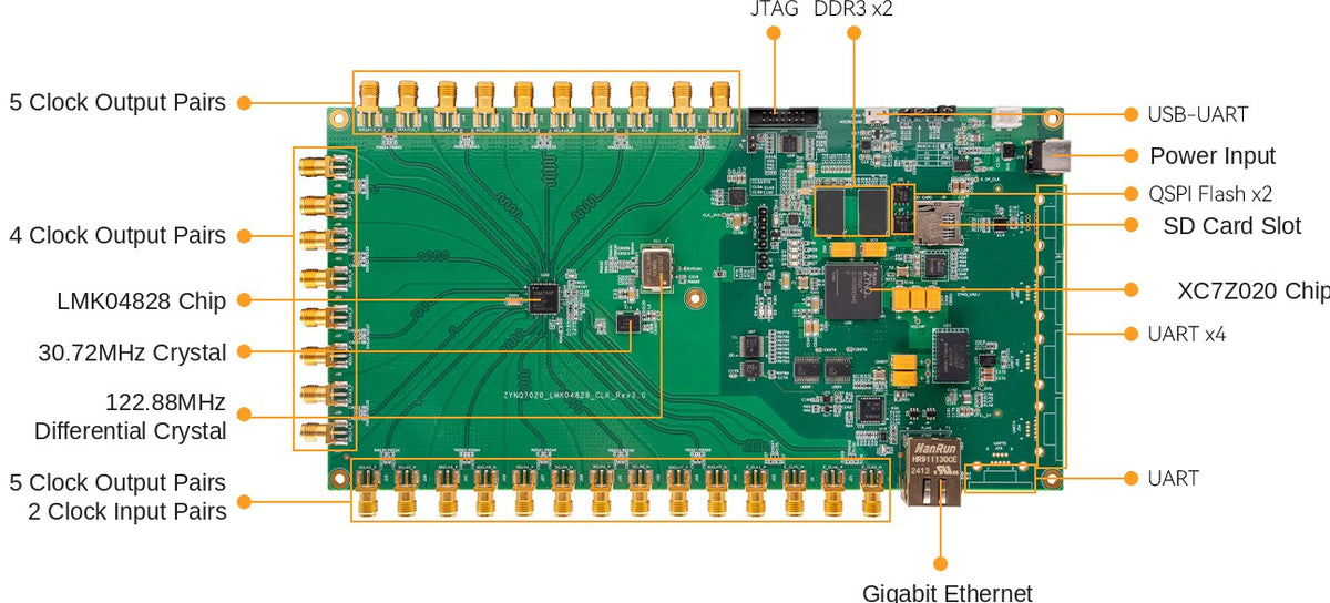
The ADK-W104 is a high-performance, highly integrated clock synchronization board built around the Xilinx Zynq-7000 XC7Z020 SoC (dual-core ARM Cortex-A9 + FPGA) and the TI LMK04828 dual-PLL, ultra-low-jitter clock generator, providing up to 14 differential clock outputs through high-performance SMA connectors. Output frequencies are programmable from 0.1 Hz to 3 GHz with typical RMS jitter of 88 fs or less, and the board supports JESD204B Subclass 1 SYSREF generation and device clocking. A 122.88 MHz differential crystal and a 30.72 MHz TCXO provide the reference, and external reference input/output supports cascaded, coherent multi-board synchronization. The board delivers a clean, precisely synchronized clock source for demanding RF and digital systems, speeding the path from prototype to production.
Specifications
| Item | Specification |
|---|---|
| FPGA | |
| FPGA | XC7Z020-2CLG400I |
| CPU | Dual-core ARM Cortex-A9 (up to 766 MHz) |
| Speed grade | -2 |
| Temperature grade | Industrial, -40°C to +85°C |
| Logic cells | 85K |
| LUTs | 53,200 |
| DSP slices | 220 |
| Block RAM | 4.9 Mb |
| Flip-flops | 106,400 |
| Clock and Synchronization | |
| Clock generator | TI LMK04828 (dual PLL, ultra-low jitter) |
| Differential outputs | 14 channels (SMA-KHDC3 high-performance connectors) |
| Output frequency range | 0.1 Hz to 3 GHz (programmable) |
| RMS jitter (12 kHz to 20 MHz) | ≤ 88 fs (typical) |
| JESD204B support | Subclass 1, SYSREF generation, device clock |
| Reference oscillators | 122.88 MHz differential crystal (OSCIN) + 30.72 MHz TCXO |
| Multi-board synchronization | External reference input/output, cascaded coherent operation |
| Memory and Interfaces | |
| DDR3 memory | 2x 1GB DDR3 on the PS side, 2GB total, 32-bit bus |
| QSPI Flash | 2x 32MB QSPI Flash, 64MB total, for FPGA user data storage |
| SD card slot | Micro SD, SDIO mode, for Linux boot |
| Ethernet | 1x PS-side Gigabit Ethernet interface |
| UART | 5x PL-side UART interfaces via J30J connector |
| USB UART | 1x PS-side USB-UART interface, for serial debugging and data communication |
| JTAG | 14-pin JTAG port, for FPGA program download and debugging |
| GPIO | 4x PL GPIO interfaces |
| LED | 4x PL LEDs |
| Power and Dimensions | |
| Power input | 12V |
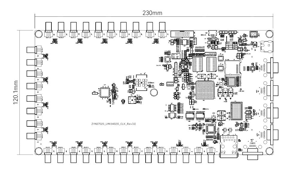
| Dimensions | 230 mm x 120.1 mm |
What’s in the box
- Clock synchronization board x 1
- SD card x 1
- Power adapter x 1
- Power cord x 1
Share