Wideband RF Transceiver FMC HPC Module ADK-9000
Wideband RF Transceiver FMC HPC Module ADK-9000
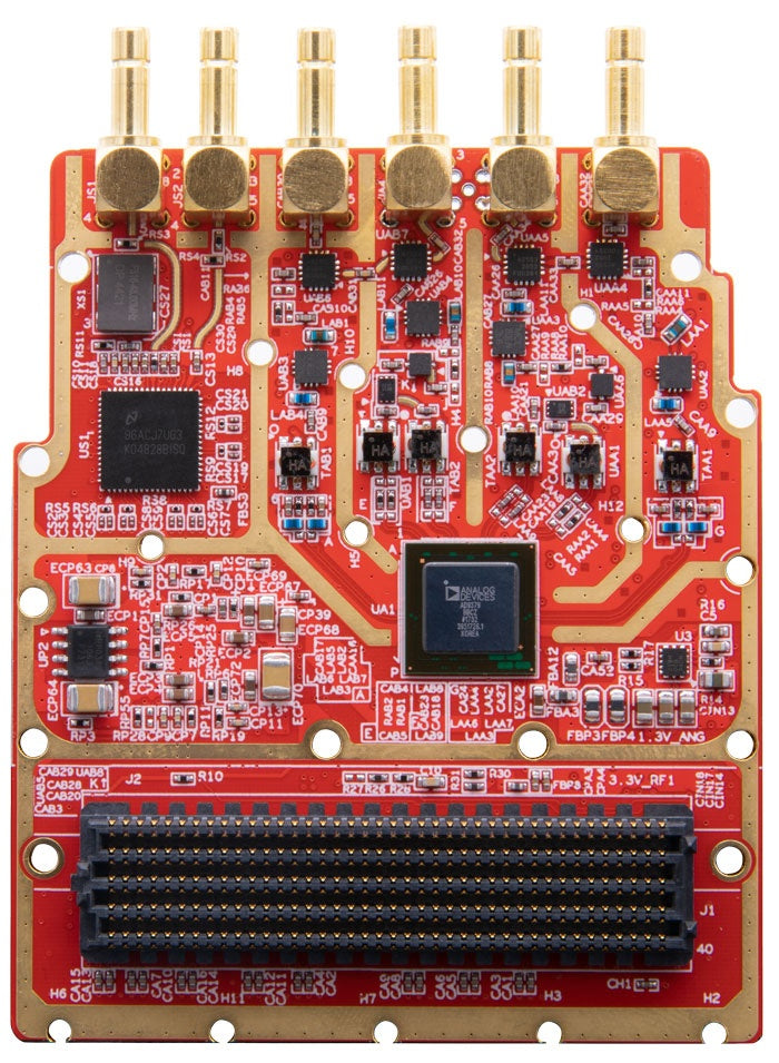
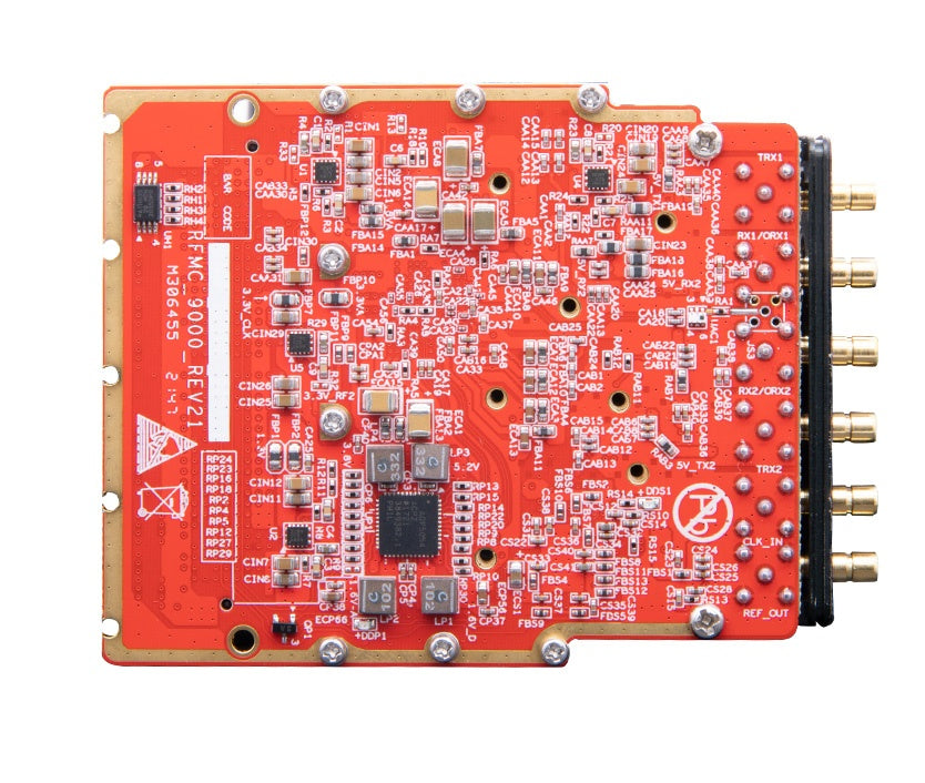
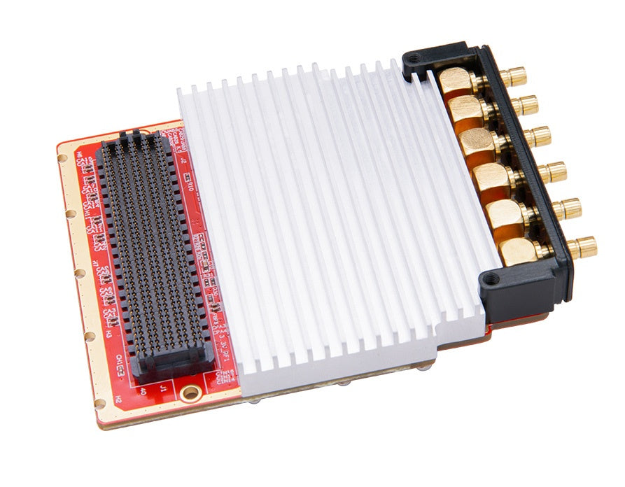
The ADK-9000 is a highly integrated RF FMC daughter card for general-purpose software-defined radio platforms. It covers the 75 MHz to 6 GHz frequency range and integrates a dual-channel transceiver link, with a maximum transmit real-time bandwidth of 450 MHz and a receive bandwidth of 200 MHz.
The RF transceiver chip fitted to this module is either the AD9009 or the AD9379: the manufacturer specification states that the two chips are shipped randomly, so the specific chip fitted is not selectable.
The RF front end includes a power amplifier, antenna switches and balun components. On the transmit path a power amplifier (PA) is added; on the receive path a low-noise amplifier (LNA) provides 15 dB of external link gain (300 MHz-6 GHz). Dual on-board antenna switches support TDD and FDD mode switching with IO control, nanosecond-level switching speed and 40 dB isolation for a single switch. Clocking is built around the TI LMK04828 clock chip, providing a flexible, variable reference clock and support for dynamic JESD204B sampling clock rates. The functional block diagram labels the transceiver block ADRV9009 and the clock chip LMK04828.
Specifications
| Item | Specification |
|---|---|
| Model | ADK-9000 |
| Transceiver chip | AD9009 or AD9379 (the two chips are shipped randomly, per the source specification) |
| Resolution | 16bit ADC & 14bitADC (wording as printed in the source specification table) |
| Antenna switch | Supports TDD mode |
| Frequency coverage | 75 MHz-6 GHz |
| Bandwidth | Transmit up to 450 MHz, receive up to 200 MHz |
| Power amplifier | 14 dB @ 2 GHz; supports maximum transmit output power of 10 dBm |
| RF impedance | 50 Ω matched |
| Digital interface | JESD204B |
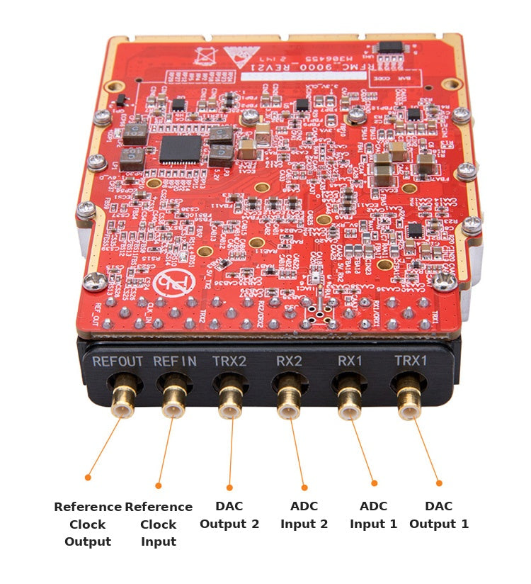
| Clock | Internal or external reference clock supported |
| FMC interface | HPC |
| Board dimensions | 76.5 x 69 mm |
RF Characteristics
| Item | Specification | Remark |
|---|---|---|
| TX Frequency | 75~6000 MHz | |
| TX Interface | SMB | |
| TX Bandwidth | Up to 450 MHz | Tx real-time bandwidth, tunable |
| TX Transmission Power | 17 dBm | 75~6000 MHz, CW |
| TX EVM | <0.7% | |
| TX Gain Control Range | 32 dB | |
| TX Gain Step | 0.05 dB | |
| TX ACLR | < -64 dBc | @10 dBm output |
| TX Spurious | 60 dBc | |
| TX SSB Suppression | 65 dBc | |
| TX LO Suppression | 70 dBc | |
| TX DAC Sample Rate (max) | 122.88 MS/s | Up to 245.76 MS/s |
| TX DAC Resolution | 14 bits | |
| RX Frequency | 75~6000 MHz | |
| RX Interface | SMB | |
| RX Bandwidth | 8 to 200 MHz | Real-time bandwidth, tunable |
| RX Sensitivity | -93 dBm @ 20 MHz | Noise Figure <3 dB |
| RX EVM | <1.2% | @-30 dBm input |
| RX Gain Control Range | 61.5 dB | Including 30 dB of ADRV9009 inside |
| RX Gain Step | 0.5 dB | |
| RX Alias Band Rejection | 80 dB | Due to digital filters |
| RX Noise Figure | <3 dB | Maximum RX gain |
| RX IIP3 (@ typ NF) | -25 dBm | |
| RX ADC Sample Rate (max) | 122.88 MS/s | Up to 153.6 MS/s |
| RX ADC Resolution | 16 bits | |
| RX ADC Wideband SFDR | 78 dBc | |
| Supply Voltage | 3.3 V & 12 V | |
| ON/OFF Time | <6 uS | TDD model |
| Duplexing Model | TDD/FDD | |
| Power Consumption | <6 W |
Note: the source page records two different transmit-power figures. Its main specification table states a maximum transmit output power of 10 dBm (power amplifier row), while its RF characteristics table lists a transmission power of 17 dBm (75~6000 MHz, CW). Both values are published above as recorded and have not been reconciled.
Warranty
The main product is covered by a 12-month warranty. FPGA chips and LCD screens are consumable parts and are not covered by the warranty. All accessories and gifts are not covered by the warranty.
Share