AMD Virtex UltraScale+ FPGA Development Board ADK-VU13G
AMD Virtex UltraScale+ FPGA Development Board ADK-VU13G
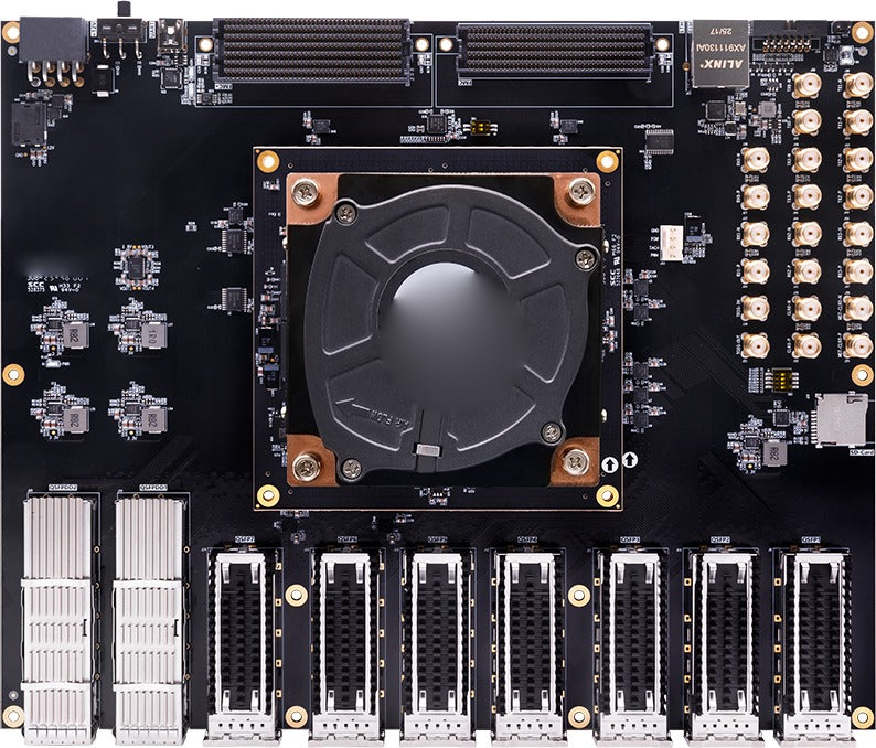
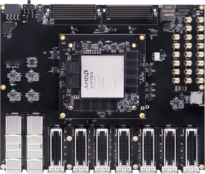
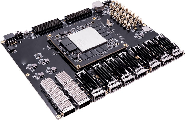
The ADK-VU13G is a high-end FPGA development and verification platform built around the AMD Virtex UltraScale+ XCVU13P FPGA (XCVU13P-2FHGB2104I), designed for the most demanding data processing, high-speed interconnect and compute acceleration challenges, and an ideal platform for researchers, algorithm engineers and system architects carrying out prototyping and product development. It combines 3,780K logic cells, 12,288 DSP slices delivering 38.3 TOP/s of peak INT8 performance, 76 GTY transceivers at 28.21 Gbps, 20GB of DDR4 memory and 256MB of QSPI flash with two 200G QSFP-DD and seven 100G QSFP28 optical ports (1.1 Tbps of total network bandwidth), FMC+ and FMC HPC expansion and PCIe Gen3 x16. Its enhanced DSP core is optimised for fixed- and floating-point computation including INT8, meeting the needs of AI inference and compute-intensive applications such as network systems above 1 Tb/s, machine learning, compute acceleration, test and measurement, and radar and early-warning systems. Application areas: compute acceleration, 5G base stations, wired communications, network acceleration, test and measurement, machine learning and AI, radar, and emulation and prototyping.
Specifications
| Item | Specification |
|---|---|
| Core board | |
| FPGA device | XCVU13P-2FHGB2104I |
| Operating temperature | Industrial grade, -40 °C to +85 °C |
| Memory | 20GB DDR4 |
| QSPI flash | 256MB |
| System logic cells | 3,780K |
| Flip-flops | 3,456K |
| Look-up tables | 1,728K |
| Max. distributed RAM | 48.3 Mb |
| Total Block RAM | 94.5 Mb |
| UltraRAM | 360.0 Mb |
| DSP slices | 12,288 |
| Peak INT8 DSP | 38.3 TOP/s |
| PCI Express | PCIe Gen3 x16 |
| 150G Interlaken | 8 |
| 100G Ethernet MAC/PCS | 12 |
| GTY transceivers | 76x 28.21 Gbps |
| HP I/O | 377 |
| Interfaces and features | |
| QSFP-DD ports | 2x QSFP-DD ports, 8 lanes each, 16 lanes total, connected to the FPGA GTY transceivers, up to 25 Gbps per lane |
| QSFP28 ports | 7x QSFP28 ports, 4 lanes each, 28 lanes total, connected to the FPGA GTY transceivers, up to 25 Gbps per lane |
| FMC+ connector | 1x standard FMC+ connector, for FMC+ and FMC modules (HDMI input/output modules, binocular camera modules, high-speed AD modules, etc.) |
| FMC connector | 1x standard FMC HPC expansion connector, for FMC daughter cards (HDMI input/output modules, binocular camera modules, high-speed AD modules, etc.) |
| Gigabit Ethernet | 1x Gigabit Ethernet port, for Ethernet data exchange with a computer or other network equipment |
| SMA input/output | 9 pairs of SMA differential connectors to the FPGA high-speed transceiver pins, plus 1 differential clock and 1 trigger signal, for high-speed transceiver and differential-pair signal verification |
| USB UART | 1x UART-to-USB interface, for communication with a computer and debugging |
| Micro SD slot | 1x Micro SD card slot, for operating-system images and file systems |
| JTAG | 1x 14-pin 2.00mm standard JTAG port, for FPGA program download and debugging |
| DIP switch | 4-position DIP switch, for simple input verification |
| LEDs | 6 LEDs: on the core board, 1 user indicator and 1 DONE configuration indicator; on the baseboard, 2 user indicators and 2 serial-port indicators |
| Button | 1x user button |
| Power | |
| Power supply | 12V / 15A |
| Input voltage | +12V |
| Input current | 15A maximum |
| Mechanical | |
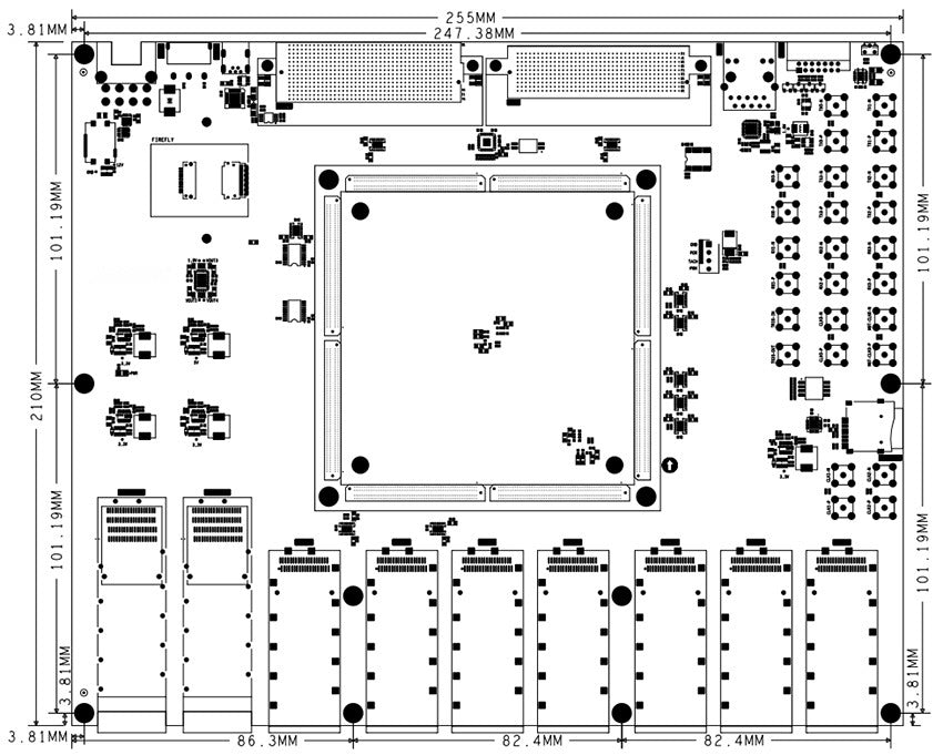
| Dimensions | 210 mm x 255 mm |
What’s in the box
- FPGA development board x 1
- USB downloader x 1
- Mini USB cable x 1
- Cooling fan x 1
- SMA cables x 6
- SMA elbows x 7
- 12V power supply x 1
- SD card x 1
Share