AMD Kintex UltraScale+ XCKU3P FPGA Development Board ADK-KU3
AMD Kintex UltraScale+ XCKU3P FPGA Development Board ADK-KU3
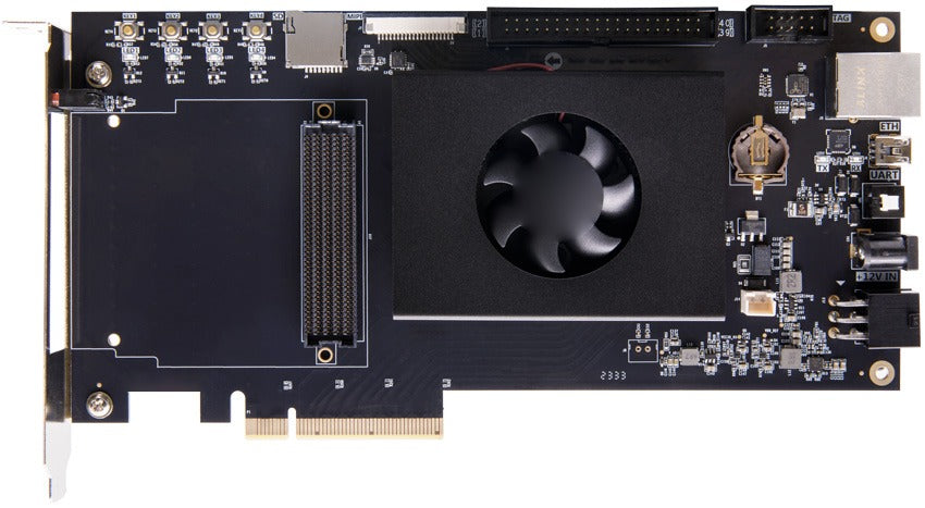
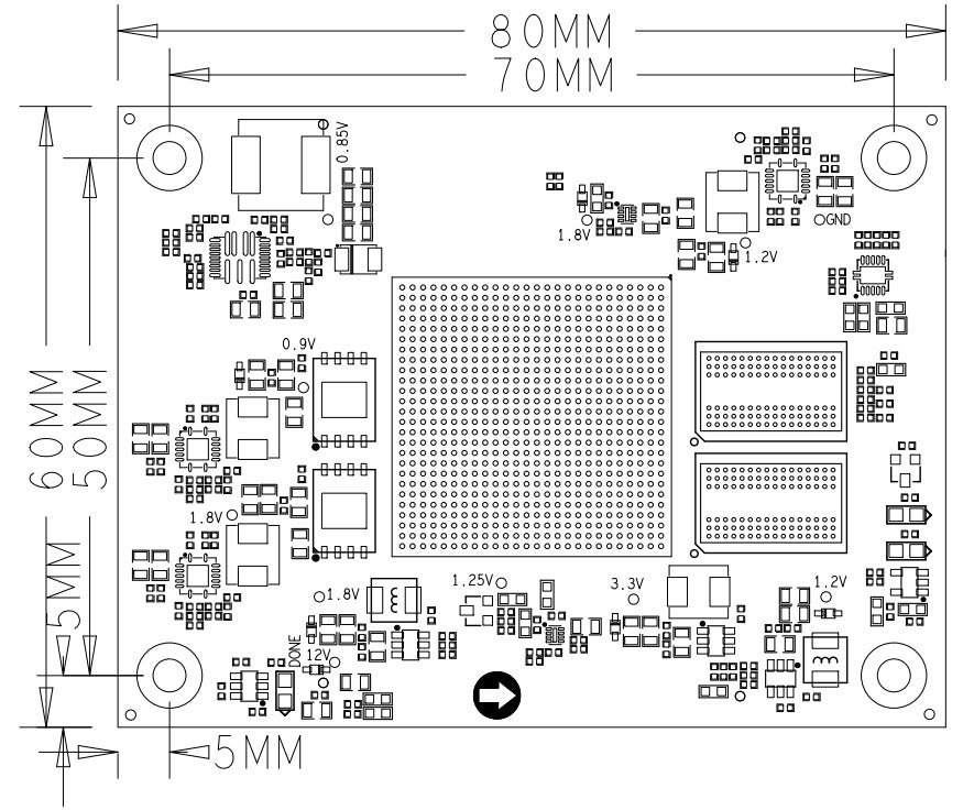
The ADK-KU3 is a high-end FPGA development board built around the AMD Xilinx Kintex UltraScale+ XCKU3P, pairing the ACKU3 core board with an expansion board. The expansion board integrates a PCIe 3.0 x8 interface, an FMC HPC connector, a MIPI Lane x4 camera input, Gigabit Ethernet and more, while the core board carries a 16 nm Kintex UltraScale+ device which, compared with 7 series FPGAs, cuts power consumption by 60%. Its GTY 28 Gb/s x16 transceivers provide a cost-effective solution for applications that need high-end features.
Eight high-speed transceivers connect to the FMC HPC interface’s dedicated high-speed pins, so FMC daughter cards such as HDMI input/output modules, high-speed AD modules, SDI input/output modules, optical fibre modules, binocular camera modules, Cameralink and GMSL camera modules can be attached for free expansion and high-speed transmission. The board suits wireless MIMO, PON access, Nx100G wired networks, data centre networking and storage acceleration, video and image processing, semiconductors, industrial control, machine vision, the Internet of Things and medical imaging.
Specifications
| Item | Specification |
|---|---|
| FPGA and Core Board | |
| Core board | ACKU3 |
| FPGA | XCKU3P-2FFVB676I |
| Operating temperature | Industrial grade (speed grade -2), -40 °C to +85 °C |
| System logic cells | 356K |
| CLB flip-flops | 325K |
| CLB LUTs | 163K |
| Max. distributed RAM | 4.7 Mb |
| Total Block RAM | 12.7 Mb |
| UltraRAM | 13.5 Mb |
| Clock management tiles | 4 |
| DSP slices | 1,368 |
| GTY transceivers | 16x 28 Gb/s |
| PCI Express | PCIe Gen3 x8 |
| HD I/O | 70 |
| HP I/O | 96 |
| Memory and Storage | |
| DDR4 | 2GB (2x 1GB DDR4 chips, 32-bit), data rates up to 2666 Mbps |
| QSPI Flash | 64MB (2x 32MB chips), storing FPGA configuration files and other user data |
| SD card slot | 1x Micro SD card slot, for operating system images and file systems |
| Oscillators | 2x 200 MHz differential oscillators, providing reference clocks for the DDR4 controller and FPGA logic |
| Interfaces | |
| PCIe interface | PCI Express 3.0 x8, up to 8 Gb/s per lane |
| FMC expansion | 1x FMC HPC interface, for FMC daughter cards such as HDMI, AD, optical fibre, SDI and binocular camera modules |
| MIPI input | 1x MIPI Lane x4 input, up to 2.5 Gb/s, for the AN5020 MIPI camera module |
| Ethernet | 1x Gigabit Ethernet interface, 10/100/1000 Mbps, full duplex and auto-negotiation |
| USB-UART | 1x UART-to-USB interface, for communication with a PC and convenient debugging |
| 40-pin expansion | 1x 40-pin 2.54mm-pitch expansion header, for add-on modules such as cameras, LCD screens and high-speed AD modules |
| JTAG | 1x 10-pin 2.54mm standard JTAG port, for FPGA system debugging and download |
| RTC | Onboard real-time clock with battery holder (CR1220 battery not included) |
| LEDs | Core board: 1 power indicator, 1 DONE configuration indicator and user LEDs; carrier board: 1 power indicator, 4 user LEDs and 2 serial-port indicators |
| Power and Dimensions | |
| Input voltage | +12V |
| Power supply | 12V / 3A |
| Input current protection | 3A maximum |
| Dimensions | 215 mm x 111 mm |
| PCB layers | Core board 14-layer PCB design; expansion board 10-layer PCB design, with dedicated power and GND layers |
What’s in the box
- Development board x 1
- Cooling fan x 1
- Mini USB cable x 1
- USB downloader x 1 set
- 12V power supply x 1
- PCIe bracket x 1
Share