AMD Kintex UltraScale XCKU095 FPGA Development Board ADK-KU095
AMD Kintex UltraScale XCKU095 FPGA Development Board ADK-KU095
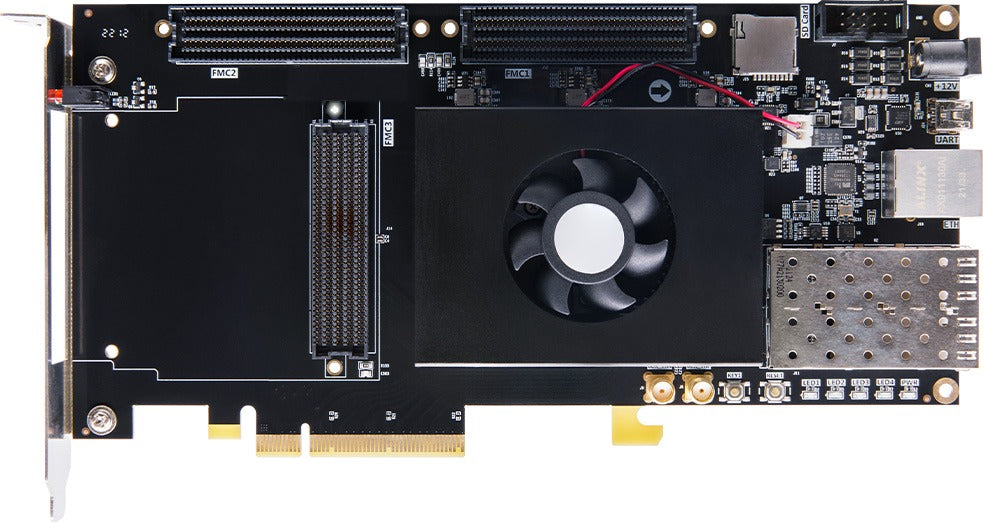
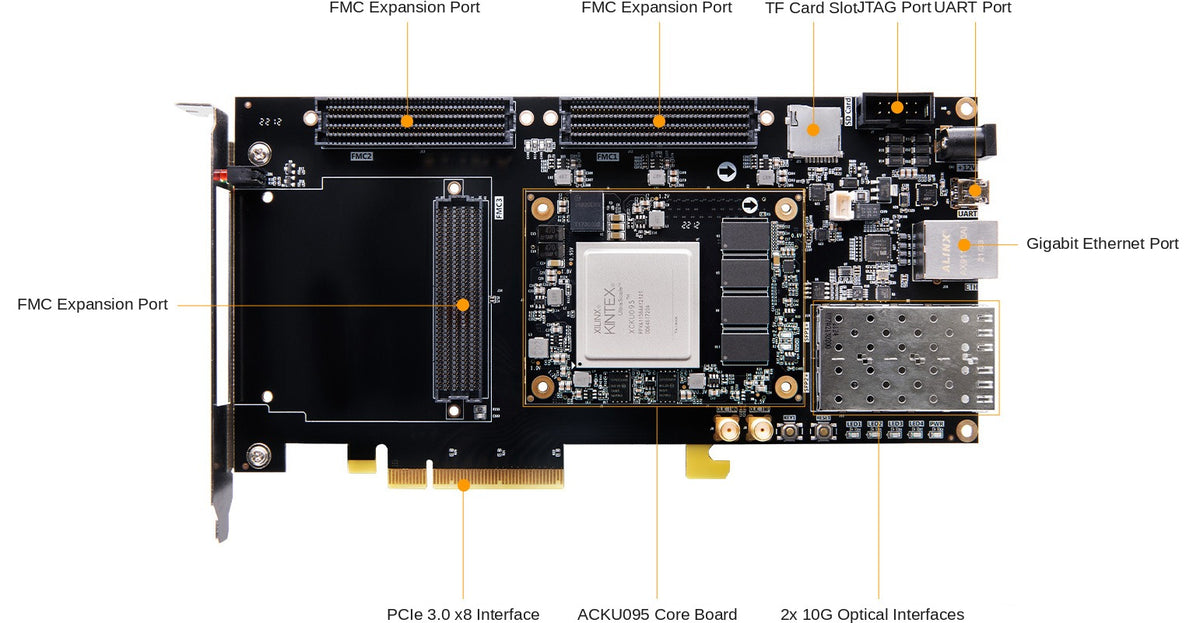
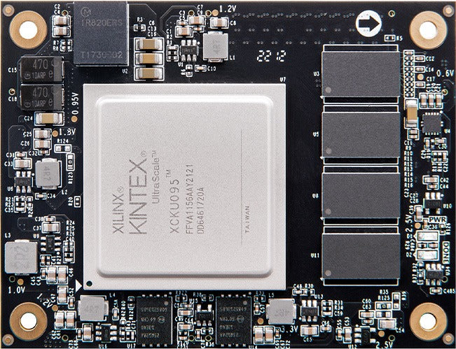
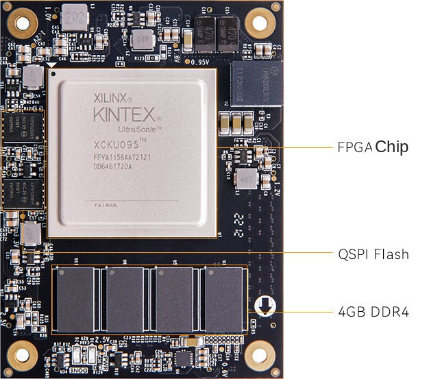
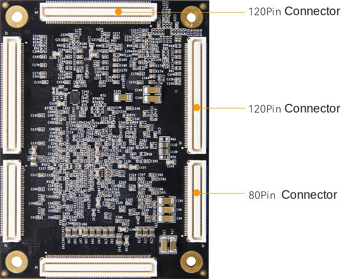
The ADK-KU095 is a high-performance FPGA development platform built around the AMD Kintex UltraScale XCKU095, offering high-speed logic processing, large memory capacity, high-performance DSP units, high-speed serial transceivers, flexible I/O interfaces and strong PCIe support. The platform combines the ACKU095 core board with a carrier (expansion) board, making it convenient for secondary development and solution verification.
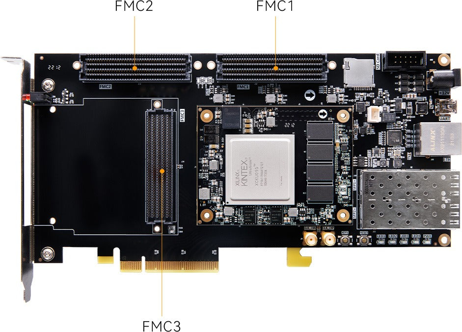
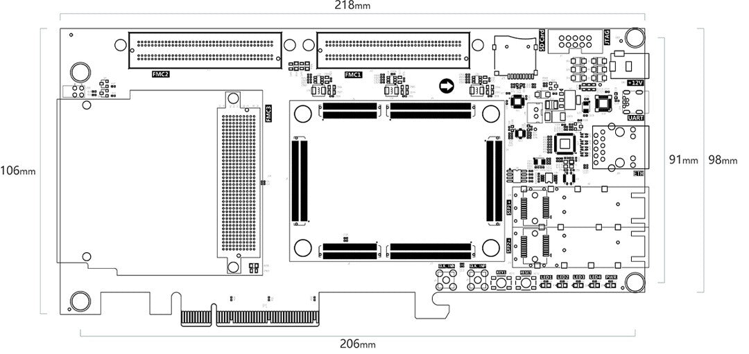
Three standard FMC expansion connectors provide 130 pairs of differential I/O signals and 9 pairs of 16.3G high-speed GTH transceivers, so a wide range of FMC modules can be attached, such as HDMI input/output modules, binocular camera modules and high-speed AD modules. With its rich interfaces and processing performance, the ADK-KU095 suits data centre computing and storage acceleration, 5G communications and network optimisation, industrial control, optical communication systems, medical ultrasound imaging and security monitoring.
Specifications
| Item | Specification |
|---|---|
| FPGA | |
| FPGA | XCKU095-1FFVA1156I |
| Grade | Speed grade -1, industrial grade, -40 °C to +85 °C |
| Logic cells | 1,176K |
| CLB LUTs | 537K |
| CLB flip-flops | 1,075K |
| Max. distributed RAM | 4,800 kb |
| Clock management tiles (CMTs) | 16 |
| Total Block RAM | 59.1 Mb |
| DSP slices | 768 |
| Transceivers | 20x 16.3 Gbps GTH |
| PCI Express | PCIe Gen3 x8 |
| HR I/O | 52 |
| HP I/O | 302 |
| Memory and Storage | |
| DDR4 | 4x 1GB DDR4 chips, 4GB total, 64-bit |
| QSPI Flash | 2x 32MB QSPI Flash, 64MB total, for FPGA user data storage |
| EEPROM | 1x EEPROM, for I2C bus communication and storing user-defined information |
| SD card slot | 1x Micro SD card interface, for FPGA read/write and storage of SD card data |
| Interfaces | |
| Optical interfaces | 2x SFP+ optical interfaces, up to 12.5 Gb/s each |
| FMC expansion | 3x standard FMC connectors (2x LPC, 1x HPC), for FMC daughter cards such as HDMI input/output modules, binocular camera modules and high-speed AD modules |
| PCIe interface | 1x PCIe 3.0 x8 interface, for PCIe data communication with a PC |
| USB-UART | 1x UART-to-USB interface, for communication with a PC and convenient debugging |
| Ethernet | 1x 10/100/1000M Ethernet RJ45 interface |
| SMA | 2x SMA external interfaces, pins connected to ordinary clock signals, for external input/output signals |
| Oscillator | 1x onboard 200 MHz clock source providing the system clock for the FPGA |
| JTAG | 1x 10-pin 2.54mm standard JTAG port, for FPGA program download and debugging |
| Temperature sensor | 1x LM75A temperature sensor chip, detecting the ambient temperature |
| LEDs | 1x power indicator, 4x user indicators, 2x panel indicators |
| Buttons | 1x reset button, 1x general-purpose button connected to an FPGA I/O |
| Power and Dimensions | |
| Input voltage | +12V |
| Power supply | 12V / 3A |
| Input current protection | 3A maximum |
| Dimensions | 210 mm x 106.65 mm |
| PCB layers | Core board 18-layer PCB design; expansion board 12-layer PCB design, with dedicated power and GND layers |
What’s in the box
- Development board x 1
- Cooling fan x 1
- Mini USB cable x 1
- USB downloader x 1
- 12V power supply x 1
Share